Analysis of DCDC Boost Circuit
2024-11-01 09:40
Analysis of DCDC Boost Circuit
In the previous issue, we introduced the working principle and duty cycle calculation of DCDC Buck circuit. In this issue, we will introduce DCDC Boost circuit.
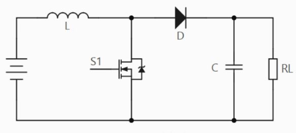
Boost voltage is a non isolated DC converter with an output voltage greater than or equal to the input voltage, consisting of inductors, capacitors, diodes, and switching devices. As shown in the following figure.

Boost circuit
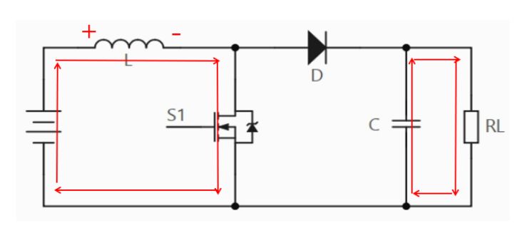
Assuming that switch S1 has been disconnected for a long time, all components are in an ideal state, and the capacitor voltage is equal to the input voltage. During the charging process, switch S1 is closed. At this point, the input voltage flows through the inductor, and the diode prevents the capacitor from discharging to ground. Due to the input being direct current, the current on the inductor increases linearly at a certain ratio, which is related to the size of the inductor. As the inductor current increases, some energy is stored in the inductor. When the circuit works stably, the capacitor stores a certain amount of energy and supplies power to the load. At this time, the induced voltage of the inductor is left positive and right negative, and the current flow direction is shown in the following figure.

When S1 is closed, the current flows in the circuit
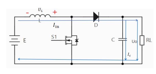
When switch S1 is turned off, due to the inability of the inductor's current to suddenly change, the current on the inductor decreases linearly, while the inductor charges the capacitor and supplies power to the load. At this time, the induced voltage of the inductor is left negative and right positive. The inductor and the power supply are connected in series in the forward direction, and the output voltage Uo=+E is used to achieve the boost function. The current flow direction is shown in the following figure.

When S1 is disconnected, the current flows in the circuit
When switch S1 is turned on, the power supply charges the inductor, and at this time, the voltage of the inductor![]() =E,inductor current
=E,inductor current![]() =
= ![]() =
=![]() ,The current does not flow through the diode, and the current of the diode is 0 at this time,The current flowing through the capacitor is
,The current does not flow through the diode, and the current of the diode is 0 at this time,The current flowing through the capacitor is![]()
When switch S1 is disconnected, the inductor charges the capacitor and supplies power to the load. At this time, the voltage across the inductor is![]() =
=![]() ,The inductor current is
,The inductor current is![]() =
= ![]() ,
,![]() =
=![]() ,
,![]() ,Capacitive current
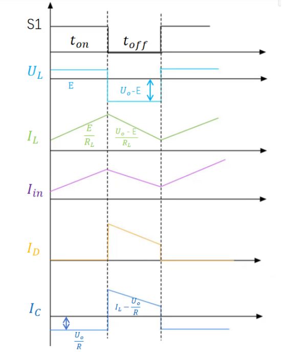
,Capacitive current![]() 。The current changes of each component in the specific circuit are shown in the following figure.
。The current changes of each component in the specific circuit are shown in the following figure.

Analysis diagram of current of each component during the operation of the boost circuit
Calculation of duty cycle of boost circuit:
According to the volt second of inductance (as introduced in the previous issue)
E×![]() ×
×![]() = 0
= 0
Organized as:![]() =
=![]()
of which,![]() ,D is the duty cycle of the boost circuit, so
,D is the duty cycle of the boost circuit, so![]() =
=![]() ×E,Therefore, the boost circuit also controls the output voltage by controlling the duty cycle of the switching transistor.
×E,Therefore, the boost circuit also controls the output voltage by controlling the duty cycle of the switching transistor.
The above is all about DCDC circuits. Thank you for reading!
Prev:


