Different switches | Different processes and characteristics of MOS tubes
2024-04-01 16:47
The previous article explained the working principle of MOS tubes and also preliminarily demonstrated the structure of MOS tubes; today's topic is the different processes and characteristics of MOS tubes. This article will describe several common processes on the market: VDMOS (vertical conductive double diffused field effect transistor), Trench MOSFET (trench type), SGT MOSFET (shielded gate trench) and SJ MOSFET (super junction).
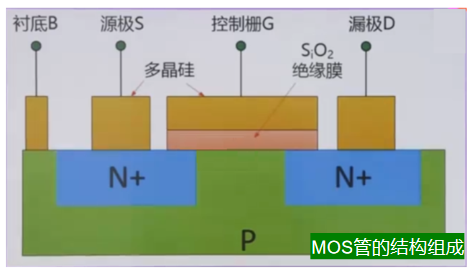
The most common and typical planar gate structure of MOSFET includes the following main parts:

Figure 1
Gate: It is the control element of MOSFET, used to control the opening and closing of the channel, corresponding to one pin.
Source: It is the source of electrons at the input end of MOSFET, corresponding to one pin.
Drain: It is the outlet of electrons, corresponding to one pin.
Substrate: The substrate is the bottom material of MOSFET, which provides carriers for the conductive channel of MOSFET.
Oxide Insulator: Usually SiO2, placed between the source and drain regions and the gate for insulation.
1. Vertical Conductive Double Diffused Field Effect Transistor (VDMOS)
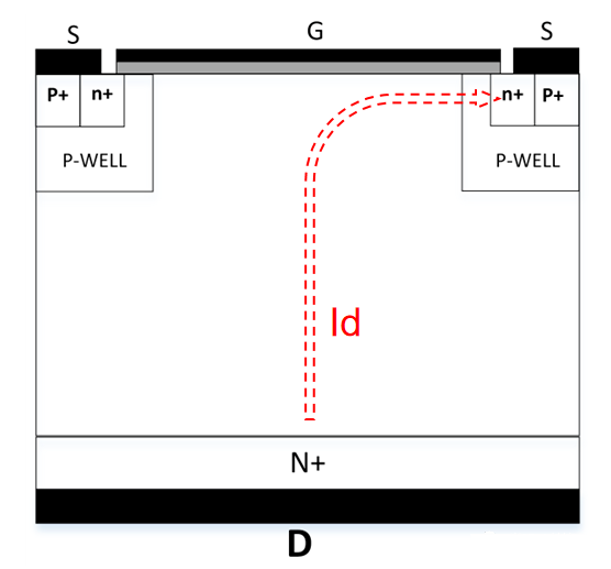
In the VDMOS structure, the drain end is not in the same plane as the source end and the gate end (Figure 2).

In the VDMOS structure, the channel is vertical and the gate is planar. This design has the following advantages:
·Higher voltage resistance: The vertical channel can withstand higher voltage, thereby improving the voltage resistance of the MOSFET.
·Smaller area: The vertical channel makes the MOSFET area smaller, and the finished product package volume can be smaller.
·Lower parasitic capacitance: The vertical channel can make the gate metal area of the MOSFET smaller and the parasitic capacitance lower, thereby increasing the switching speed.
2. Trench MOS (trench type)
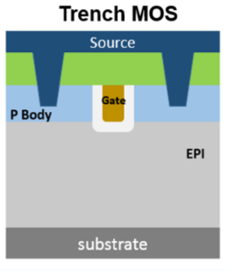
The gate of the trench MOS is a trench dug inward, and then silicon oxide is filled in the trench. This process is called gate oxidation.

Figure 3
Compared with the planar gate MOSFET, the trench gate MOSFET passes through the bottom of the P-type base region by constructing a trench structure. The formed channel is located between the N+ source and the N drift region, eliminating the JFET region and the JFET resistance. Therefore, the total characteristic resistance is greatly reduced compared to the planar gate structure.
3. SGT MOS (shielded gate trench)
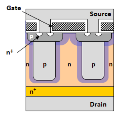
SGT-MOS is an improved structure of Trench MOS, which is usually suitable for medium and low voltage scenarios (as shown in Figure 4). Compared with the traditional Trench MOSFET, SGT-MOSFET adds a polysilicon electrode under the gate electrode, namely the shielding electrode or coupling electrode. The shielding electrode is connected to the source electrode, which realizes the function of shielding the gate and the drift region, reduces the Miller capacitance, and speeds up the switching speed of the device. At the same time, it realizes the charge coupling effect, reduces the critical electric field strength of the drift region, reduces the on-resistance of the device, and reduces the switching loss.

Figure 4
4. SJ MOS (Super Junction)
In terms of power MOS, compared with the conventional VDMOS device structure, RDS(on) and BVSS have a contradictory relationship. To improve BVSS, it is generally necessary to reduce the EPI doping concentration (Epi doping refers to depositing a layer of doping material on the surface of the wafer to change the conductive properties of the wafer. By controlling the type and concentration of the doping material, the electrical properties of the wafer can be precisely controlled). However, the epitaxial layer is also a channel for the flow of forward current. If the EPI doping concentration is reduced, the resistance will inevitably increase, and RDS(on) will increase. Otherwise, it is necessary to increase the chip area, increase the package size, and increase a lot of production costs. Therefore, for ordinary VDMOS, the contradiction between the two is irreconcilable.
The high-voltage power MOSFET using the super junction (Super Junction, referred to as SJ) process is to set a P column area deep into the EPI layer, and to increase the doping concentration of the current conduction area to significantly reduce the on-resistance per unit area, but at the same time, the withstand voltage is not affected, making it a new type of device with high withstand voltage and low resistance characteristics. The structure diagram is shown in Figure 5. The special super junction structure reduces the internal resistance of the high-voltage super junction MOSFET to 1/5 of that of the traditional planar MOSFET under the same area, and the switching loss is reduced to 1/2 of that of the ordinary VDMOSFET.
Compared with the traditional power MOSFET, SJ-MOSFET has the advantages of low conduction loss, large current driving capability, low gate charge, low turn-on voltage, and fast switching speed.

Figure 5
5. Summary
To sum up, the advantages and disadvantages of MOS tubes of various processes are as follows:
VDMOS
Advantages: high withstand voltage, smaller area with the same specification, low parasitic capacitance.
Disadvantages: large on-resistance and large leakage current.
Trench MOS
Advantages: small on-resistance, small parasitic capacitance, excellent switching performance.
Disadvantages: cannot withstand high voltage, often used in low-voltage fields below 100V, weak impact resistance.
SGT MOS
Advantages: small Miller capacitance, low switching loss, low conduction loss, often used in medium and low voltage fields (about 200V).
Disadvantages: complex process and high cost.
SJ MOS
Advantages: small internal resistance, small gate charge, fast switching speed, often used in high voltage fields (600-800V).
Disadvantages: weak surge resistance.
The above-mentioned MOS production lines represented by Yachuang are all covered, such as Huayiwei, LRC, Xinjie Energy, Yangjie, ROHM, and Toshiba. You can recommend as needed.
Due to limited space, there are many improvements and derivative processes of MOS tubes. This article will only introduce several mainstream ones for the time being. If you have different opinions, please feel free to communicate in the comment area!


