Different switches丨The working principle of MOS tube
2024-03-15 16:53
Last time, I introduced the triode that can be used as a switch and has an amplifying effect. I believe that after the explanation in the previous article, everyone has a specific understanding of the switching function of the triode. However, in some application scenarios, because the triode is a current-controlled switch, power consumption needs to be generated during the opening process of the triode, and in some high-voltage or low-noise demand circuits, the application of the triode is always unsatisfactory. At this time, the protagonist of this article, MOSFET, is needed.
MOS is the abbreviation of MOSFET. MOSFET Metal-Oxide-Semiconductor Field-Effect Transistor, referred to as Metal-Oxide-Semiconductor Field-Effect Transistor (MOSFET).
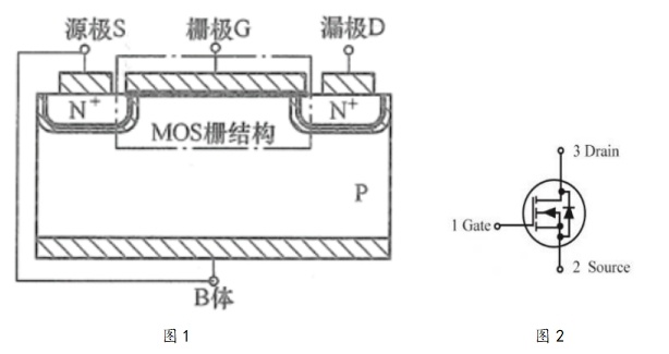
Like the triode, the MOS tube also has three poles, which are the gate, source and drain. The specific structure is shown in the figure below:

Figure 1 shows the typical internal structure of Nmos, where the source is generally directly connected to the substrate. At this time, a body diode is formed between the DS poles (such as the diode in the middle of the DS poles in Figure 2), which means that when the current can be directly conducted from the PN junction direction of S→D. However, when a normal MOS is used as a switch, the D pole will have a higher potential than the S pole, and the body diode is in a reverse cutoff state. The gate G of the MOS tube is a thin metal sheet that has no direct contact with the P junction of the MOS. At this time, if a voltage is applied between the G pole and the S pole, the electrons of the P junction will be affected by the electric field and attracted between the two N junctions, thereby forming a conductive channel between the DS. The specific working principle can be seen in Figure 3.

Figure 3
Then after the whole process, the MOS tube has truly achieved the purpose of switching.
Through this process, we can also roughly analyze some key parameters of MOSFET.
First, the withstand voltage of MOSFET: Based on the above MOS structure description, we can understand that the withstand voltage of MOS is actually the reverse breakdown voltage of the body diode, which is the VDSS in the specification book.
Secondly, the withstand current ID of MOSFET is the current that this conductive channel can withstand at the maximum power. When the current exceeds the specification, the MOSFET will heat up sharply, eventually leading to the burning of the MOSFET. In practical applications, leaving enough margin and maintaining good heat dissipation of MOSFET can greatly enhance the stability of MOSFET operation.
Third, we know that the metal sheet of the gate S is actually not in contact with the P junction, so there will be a parasitic capacitance Ciss between the two, also called input capacitance, and this capacitance directly affects the speed of the conductive communication, that is, the switching speed of MOSFET. We know that the larger the capacitance, the longer the charging time, and the smaller the capacitance, the shorter the charging time. Therefore, in the selection of MOSFET, if the MOSFET needs high-frequency switching, then the smaller this parameter, the better.
Fourth, when the conductive channel is formed, a parasitic resistance RDS (on) is bound to be generated. This resistance usually ranges from a few milliohms to a few ohms. If the MOS is in the on state for a long time, the smaller the resistance value is, the smaller the overall heat generation and power consumption of the MOSFET will be.
Therefore, in the selection and replacement of MOS, in addition to parameters such as voltage and current resistance packaging, it is also necessary to pay attention to the Ciss or RDS (on) of the customer's original model. If the input capacitance is small and the RDS (on) is large, then this MOS is mostly used for frequent switching in the circuit; otherwise, the main working state of the MOS is on, and it is not too sensitive to the switching speed requirements.
The above is the explanation of the working principle and parameters of the MOS tube in this issue. The application of MOSFET is quite extensive. Due to the length of the article, it has not been fully described. It will be updated in the future. If you have different opinions, you can also actively comment. I look forward to your attention.


